
Examining the Lives of Buffalo Soldiers in Italy
4 min read


What does friction have to do with processors and memory chips for computers, tablets, and smartphones? A lot actually. Friction and wear, even at the atomic level, have a big impact on the production of the semiconductor chips that power our most essential devices. Friction causes stresses and deformations that are starting to limit our ability to produce smaller and more powerful chips.
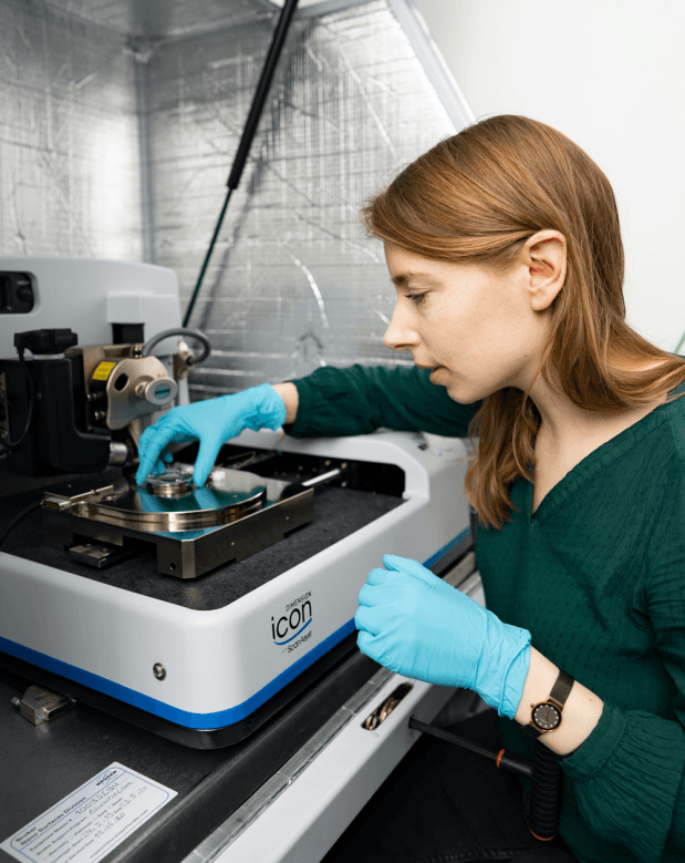
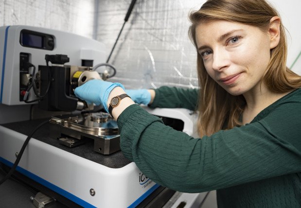
Enter Fiona Elam, a postdoc in the Contact Dynamics lab at ARCNL, the Advanced Research Center for Nanolithography (ARCNL) in Amsterdam. Fiona works on nanotribology, the science of friction, wear, and lubrication on a nano scale. At ARCNL she investigates the friction and wear that occurs during the computer chip fabrication process.
Computer chips are printed in bulk on 30cm silicon wafers. The wafers are covered with a light sensitive film and then placed onto a wafer table where they’re exposed to either UV or extreme UV light. Layers and layers of patterns are fabricated onto a single wafer to create the billions of transistors that together form integrated circuits or chips. The individual components of the transistors are tiny, just 10-14 nanometres wide (which is only a few tens of atoms.) Since the nanolithography process is happening on such a tiny scale, it’s imperative that the wafer is perfectly aligned on the wafer table. If the wafer is off by even a nanometer, the printed transistor layers won’t be stacked properly and the resulting chips will have a lower processing power.
In the Contact Dynamics lab, Fiona and her colleagues simulate the wafer-on-wafer-table interaction as it happens in an industrial setting. They are trying to predict and stabilize the friction between the wafer and the table to prevent uneven wearing. At the moment, she’s working on a project that aims to simulate certain environmental conditions found at the wafer-on-wafer table interface in immersion lithography machines. In immersion lithography, there is a film of water between the final lens and the wafer, making it possible to print smaller than normal features due to the refractive index increase with respect to air. However, the humid environment and static electricity created during the lithography process are thought to potentially corrode the wafer table. Understanding how the wafer table surface behaves both chemically and physically in corrosive environments can lead to solutions for predicting and controlling wafer table wear.
A connection to the nanolithography industry is crucial for this kind of applied research. Students and researchers at ARCNL are fortunate that the institute has an industrial partner in ASML, a Dutch company that is the world’s largest supplier of high tech lithography machines for chip making. ARCNL is actually a public-private partnership between two universities in Amsterdam (University of Amsterdam and Vrije Universiteit Amsterdam), the Dutch Research Council (NWO) and ASML. ARCNL’s close relationship with ASML offers postdocs like Fiona valuable opportunities to work directly with industry. The Contact Dynamics group is one of the research groups that works most closely with ASML and one of the group’s two leaders works part time at the company.
ARCNL’s direct connection to industry was very appealing to Fiona and influenced her decision to do a postdoc at the institute. “Since leaving university, I've always known that I want to do something more applied and see the benefit of what I’m working on in a real life situation,” she says. Both her master’s and PhD had industry partners (SKF, a Swedish bearing and seal manufacturing company, and Fujifilm respectively) and it was something she was keen to continue in her postdoc. “It's nice to have this close link with industry to be able to contribute in a meaningful way to something that will eventually help people.”
The resources of ARCNL ensure Fiona is able to conduct research that will have an impact.
“The equipment that we have here at ARCNL is top of the range,” she says. “We’re also very fortunate to have access to the Dutch NanoLab at AMOLF. We're not limited in terms of what we can do.”
ARCNL’s technical staff are another asset of the institute. They are always on hand to help and are very knowledgeable about all the in house equipment at ARCNL.
Fiona also considers the institute’s location in Amsterdam to be a plus for international researchers since the city is “a very easy place for foreign people to live” and the Dutch are very welcoming. “This is a unique place for people interested in the semiconductor industry to work,” she adds, and encourages those who want to do applied research in a friendly, international environment to apply.


| Title | Why Does Friction Limit Our Ability to Make Smarter Computer Chips? |
| Posted on | Mar 13, 2020 at 02:26 pm. |
| Category | Inspiring Ideas |
| Tags | Engineering Physics, Materials Chemistry, Materials Engineering, Materials Physics, Mechanical Engineering, Mechanics, Surface Chemistry |


